
This post is also available in:
![]() 简体中文 (Chinese)
简体中文 (Chinese)
TSMC is considering establishing advanced packaging production capacity in Japan to help Japan restart the semiconductor industry.
The company will introduce wafer substrate chip packaging technology to improve processing capabilities, save space and reduce power consumption.
At present, the investment scale and timetable have not been determined. TSMC declined to comment.
The Japanese government generously subsidizes TSMC’s plan, considering semiconductors vital to its economy. In addition, Intel is also considering establishing a packaging research institution in Japan to deepen its ties with local supply chain companies. Samsung is also establishing a packaging research facility in Yokohama and is preparing to cooperate with Japanese and other regional companies.
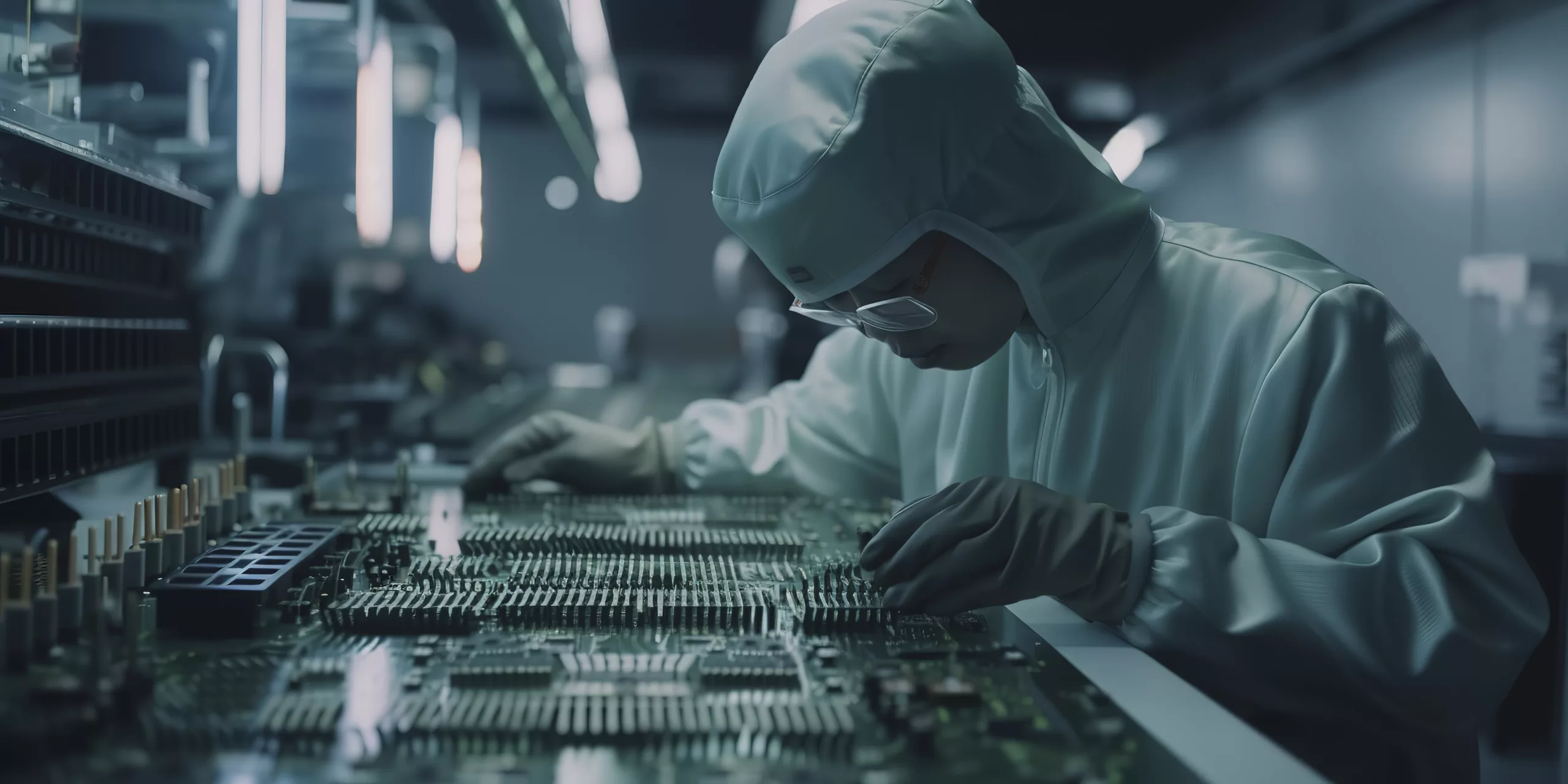
(Source: reuters Image source: freepik)